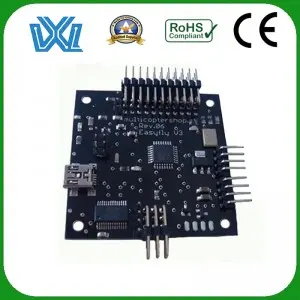
In today’s digital age, keyboards have become an essential tool for communication, programming, and gaming. The complex design of a keyboard involves various components, one of the most critical being the printed circuit board (PCB). Understanding how to design a keyboard PCB is crucial for hobbyists and professionals alike. In this blog post, we’ll delve into the complex world of keyboard PCB design to provide you with a comprehensive guide to mastering this art form.
1. Understand the basics of keyboard PCB design:
Before delving into the intricate details of keyboard PCB design, it’s important to be familiar with the basic principles. The keyboard PCB acts as a central hub connecting various switches, diodes, and other components. It provides keystroke data to the computer, enabling the user to enter commands. Understanding electrical schematics, switch matrix design, and firmware integration are critical to creating an efficient and fully functional keyboard PCB.
2. Choose the right components:
Choosing the correct components for your keyboard PCB is critical to ensuring its reliability and performance. Proper selection of switches, diodes, capacitors, resistors, and microcontrollers play an important role in determining the overall typing experience and functionality. Researching and experimenting with different components will help you find the perfect combination for your specific requirements.
3. Plan the keyboard layout:
Keyboard layout is an important aspect of PCB design. Determining the number of keys, their location, and the overall structure of the keyboard layout should be carefully considered. Factors such as ergonomics, key accessibility and usage patterns should be considered during the planning stage. Tools such as Keyboard Layout Editor (KLE) can help visualize and finalize keyboard layout designs.
4. Circuit design:
Once the keyboard layout is finalized, the next step is to design the circuit schematic. Creating an accurate circuit schematic involves connecting switches, diodes, and other components in a logical manner. Tools such as EAGLE, KiCad or Altium Designer can help create visually appealing and well-organized circuit schematics.
5. Implement PCB design:
After completing the circuit schematic, the next step is to translate it into an actual PCB design. Use PCB design software such as EAGLE, KiCad or Altium Designer to convert circuit schematics into PCB layouts. Correct component placement, efficient routing, and adhering to design guidelines are critical. Paying attention to factors such as electrical noise, ground planes, and heat dissipation will ensure that the keyboard PCB is strong and reliable.
6. Test and iterate:
Once the PCB design is complete, it is critical to test the prototype thoroughly. Checking functionality, keystroke accuracy, and signal integrity will help identify potential problems. Iterating the design based on user feedback and performance analysis is critical to achieving a high-quality keyboard PCB.
Designing a keyboard PCB is a complex but rewarding process. Mastering this art form requires a deep understanding of keyboard components, circuit design, and meticulous attention to detail. By following the steps outlined in this comprehensive guide, you can begin the journey of creating your own custom keyboard PCB. So get ready, unleash your creativity and let your fingers dance on your own masterpiece!
Post time: Sep-27-2023