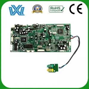
Are you a budding electronics enthusiast looking to dive into the world of PCB design? Look no further! In this beginner’s guide, we’ll explore the basic steps of designing a PCB using the popular software OrCAD. Whether you are a student, hobbyist or professional, mastering PCB design will open the door to endless possibilities. So, let’s get started.
1. Know the basics:
Before diving into the design process, familiarize yourself with the basics of PCBs. PCB is the abbreviation of printed circuit board, which is an important part of electronic equipment. It mechanically supports and electrically connects various electronic components. Solid understanding of circuit schematics, components and their layout.
2. Select OrCAD:
OrCAD from Cadence Design Systems is a leading software tool widely used for PCB design. It provides a complete set of tools for schematic capture, component placement and routing. Download and install the OrCAD software on your computer to get started.
3. Schematic capture:
Start your design journey by creating a schematic with OrCAD Capture. This tool allows you to draw circuit connections, add components and define their electrical properties. Ensure correct symbol selection and connections between individual components.
4. Component placement:
Once the schematic is complete, move on to the next step: component placement. OrCAD PCB Designer provides tools for placing components on a PCB layout. Consider factors such as component proximity, signal integrity, and optimized trace length when placing components. Strategic placement ensures efficient routing and reduces potential signal interference.
5. Routing:
Now is the most critical link in PCB design – the routing stage. OrCAD’s routing capabilities allow you to create copper traces that connect various components on a PCB. Proper routing ensures signal integrity and minimizes noise and interference. Design rules such as clearance spacing and trace thickness must be followed to ensure proper functionality.
6. Signal integrity and DRC check:
Use OrCAD’s built-in SI tools to perform signal integrity (SI) checks before finalizing your design. These checks identify potential signal interference or reflections that could affect overall performance. Also, run a design rule check (DRC) to ensure compliance with manufacturing guidelines and electrical constraints.
7. Design Verification:
Once the PCB design is complete, a thorough verification process is required. Check the design for errors, including shorts, opens, or any other issues. Check for correct component labeling, text clarity, and consistency across layers. Ensuring accuracy is critical before proceeding to manufacturing.
8. Export and manufacture:
Once you are satisfied with the design, export the PCB layout to a standard format such as Gerber RS-274X. This format is widely accepted by PCB manufacturers. Generate separate files for each layer, including copper traces, solder mask, and drilled holes. Manufacturers will use these files to create the physical PCB.
Designing a PCB with OrCAD may seem daunting at first, but with practice and persistence it can become an exciting and rewarding endeavor. Remember to start with the basics, choose the right software tools, and follow a systematic approach. PCB design is a continuous learning process, so keep exploring advanced technologies while gaining experience. So why wait? Unleash your creativity and start designing your own PCBs with OrCAD today!
Post time: Sep-01-2023

