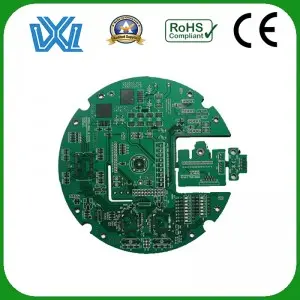
Developing a printed circuit board (PCB) can seem like a daunting task, especially for beginners. However, with the right guidance and knowledge, anyone can learn how to create their own PCB designs. In this beginner’s guide, we’ll provide step-by-step instructions on how to develop a PCB from scratch. So, let’s dive right in!
Step 1: Planning the PCB Design
Before starting the PCB development process, it is important to have a clear understanding of your project requirements. Determine the purpose of the PCB, the components it will support, and the required functionality. Create schematics to visualize circuit connections and ensure a seamless design.
Step 2: Design the PCB Layout
Once the schematic is ready, the PCB layout can be created. Choose a reliable PCB design software such as Eagle, Altium Designer or KiCad to design your board. Start by placing components strategically on the board, ensuring the shortest possible connections. Pay attention to ground planes, power routing, and signal integrity. Remember to maintain proper clearance and keep critical components away from noisy areas.
Step 3: Layout and Trace Placement
Routing involves creating the copper traces that connect components on the PCB. Place traces in such a way that noise and signal interference are minimized. Group similar components together and avoid crossing traces unless necessary. Make sure there is proper spacing between traces to prevent short circuits. If using surface mount components, make sure the traces are thin enough to accommodate the component footprint.
Step Four: Finish the Design
Thoroughly check your PCB design for accuracy and correctness. Check for any design errors, overlooked connections, or component placement errors. Use the software’s design rule checker to identify any potential problems. After everything is verified, manufacturing files are generated, including Gerber files and a Bill of Materials (BOM), to ensure accurate production of the PCB.
Step 5: Fabrication and Assembly
Send your final PCB design to the manufacturer of your choice. A variety of online PCB fabrication services provide affordable options for manufacturing your designs. Select the appropriate parameters such as sheet material, number of layers and thickness according to your requirements. Once the PCB fabrication is complete, order the necessary components and start assembling the board. Make sure to follow best soldering practices to avoid any damage to the components.
Step 6: Testing and Troubleshooting
After the PCB is assembled, it is important to test its functionality. Use a multimeter or oscilloscope to check voltage levels, signal integrity, and proper connections. Power up the PCB and test each component individually. If any issues are detected, use your debugging skills to troubleshoot them and correct accordingly.
Developing a PCB may initially seem like a complex process, but with a systematic approach and proper understanding, it becomes a manageable task. This beginner’s guide provides a step-by-step process on how to develop a PCB from planning the design to testing its functionality. As with any skill, practice and hands-on experience will further enhance your proficiency in PCB development. So dive in, take on the challenge, and let your creativity flow in designing efficient, functional PCBs. Good luck!
Post time: Aug-07-2023

