Printed circuit boards (PCBs) are an integral part of modern electronic devices, serving as the backbone of components and connections that allow electronic devices to operate efficiently. PCB manufacturing, also known as PCB fabrication, is a complex process involving multiple stages from initial design to final assembly. In this blog post, we’ll take a deep dive into the PCB manufacturing process, exploring each step and its significance.
1. Design and layout
The first step in PCB manufacturing is designing the board layout. Engineers use computer-aided design (CAD) software to create schematic diagrams showing the connections and locations of components. Layout involves optimizing the positioning of traces, pads, and vias to ensure minimal interference and efficient signal flow.
2. Material selection
PCB material selection is critical to its performance and durability. Common materials include fiberglass reinforced epoxy laminate, often called FR-4. The copper layer on the circuit board is critical for conducting electricity. The thickness and quality of copper used depends on the specific requirements of the circuit.
3. Prepare the substrate
Once the design layout is determined and materials selected, the manufacturing process begins by cutting the substrate to the required dimensions. The substrate is then cleaned and coated with a layer of copper, forming the basis for the conductive paths.
4. Etching
After preparing the substrate, the next step is to remove excess copper from the board. This process, called etching, is accomplished by applying an acid-resistant material called a mask to protect the desired copper traces. The unmasked area is then exposed to an etching solution, which dissolves the unwanted copper, leaving only the desired circuit path.
5. Drilling
Drilling involves creating holes or vias in a substrate to allow component placement and electrical connections between different layers of the circuit board. High-speed drilling machines equipped with precision drill bits can machine these small holes. After the drilling process is complete, the holes are plated with conductive material to ensure proper connections.
6. Plating and solder mask application
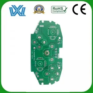
The drilled boards are plated with a thin layer of copper to strengthen connections and provide safer access to components. After plating, a solder mask is applied to protect the copper traces from oxidation and to define the solder area. The color of solder mask is usually green, but may vary based on manufacturer preference.
7. Component placement
In this step, the manufactured PCB is loaded with electronic components. The components are carefully mounted on the pads ensuring correct alignment and orientation. The process is often automated using pick-and-place machines to ensure accuracy and efficiency.
8. Welding
Soldering is the final step in the PCB manufacturing process. It involves heating elements and pads to create a strong and reliable electrical connection. This can be done using a wave soldering machine, where the board is passed through a wave of molten solder, or by manual soldering techniques for complex components.
The PCB manufacturing process is a meticulous process that involves multiple stages of transforming a design into a functional circuit board. From initial design and layout to component placement and soldering, each step contributes to the overall functionality and reliability of the PCB. By understanding the intricate details of the manufacturing process, we can appreciate the technological advances that have made modern electronic devices smaller, faster, and more efficient.
Post time: Sep-18-2023