OEM Mcpcb Manufacturers - Customized PCB Assembly and PCBA – Weilian Electronics
OEM Mcpcb Manufacturers - Customized PCB Assembly and PCBA – Weilian Electronics Detail:
Description
| Model NO. | ETP-005 | Condition | New |
| Product Type | PCB Assembly and PCBA | Min.Hole Size | 0.12mm |
| Solder Mask Colour | Green, Blue, White, Black, Yellow, Red etc Surface Finish |
Surface Finish | HASL, Enig, OSP, Gold Finger |
| Min Trace Width/Space | 0.075/0.075mm | Copper Thickness | 1 – 12 Oz |
| Assembly Modes | SMT, DIP, Through Hole | Application Field | LED, Medical, Industrial, Control Board |
About Our PCB Board Design
When we design the PCB board, we also have a set of rules: first, arrange the main component positions according to the signal process, and then follow the “circuit first difficult and then easy, component volume from large to small, strong signal and weak signal separation, high and low. Separate signals, separate analog and digital signals, try to make wiring as short as possible, and make the layout as reasonable as possible”; special attention must be paid to separate “signal ground” and “power ground”; this is mainly to prevent power ground The line sometimes has a large current passing through it. If this current is introduced into the signal terminal, it will be reflected to the output terminal through the chip, thus affecting the voltage regulation performance of the switching power supply.
Then, the arrangement position and wiring direction of the components should be as consistent as possible with the wiring of the circuit diagram, which will be much more convenient for later maintenance and inspection.
The ground wire should be as short and wide as possible, and the printed wire passing through the alternating current should also be widened as much as possible. Generally, we have a principle when wiring, the ground wire is the widest, the power wire is the second, and the signal wire is the narrowest.
Minimize the feedback loop, input and output rectification filter loop area as much as possible, this purpose is to reduce the noise interference of the switching power supply.
One-stop Solution
Inductive devices such as thermistors should be kept as far away as possible from heat sources or circuit devices that cause interference.
The mutual distance between the dual in-line chips should be greater than 2mm, and the distance between the chip resistor and the chip capacitor should be greater than 0.7mm.
The input filter capacitor should be placed as close as possible to the line that needs to be filtered.
In PCB board design, the most common problems are safety regulations, EMC and interference. In order to solve these problems, we should pay attention to three factors when designing: space distance, creepage distance and insulation penetration distance. Impact.
For example: Creepage distance: when the input voltage is 50V-250V, the L-N in front of the fuse is ≥2.5mm, when the input voltage is 250V-500V, the L-N in front of the fuse is ≥5.0mm; electrical clearance: when the input voltage is 50V-250V, L—N ≥ 1.7mm in front of the fuse, when the input voltage is 250V-500V, L—N ≥ 3.0mm in front of the fuse; no requirement is required after the fuse, but try to keep a certain distance to avoid short circuit damage to the power supply; primary side AC to DC part ≥ 2.0 mm; primary side DC ground to ground ≥4.0mm, such as primary side to ground; primary side to secondary side ≥6.4mm, such as optocoupler, Y capacitor and other component parts, the pin spacing is less than or equal to 6.4mm to be slotted; transformer two-stage ≥6.4mm or more, ≥8mm for reinforced insulation.
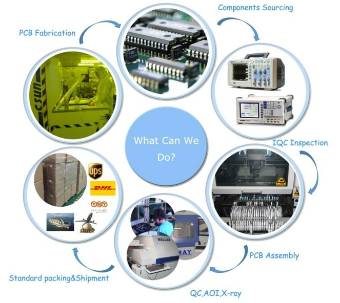
Factory Show

FAQ
Q1: How do you make sure the quality of the PCBs?
A1: Our PCBs are all 100% test including Flying Probe Test, E-test or AOI.
Q2: What is the lead time?
A2: Sample needs 2-4 working days, mass production needs 7-10 working days. It depends on the files and quantity.
Q3: Can I get the best price?
A3: Yes. To help customers control cost is what we are always trying to do. Our engineers will provide the best design to save PCB material.
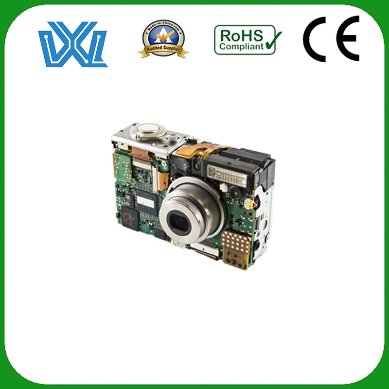
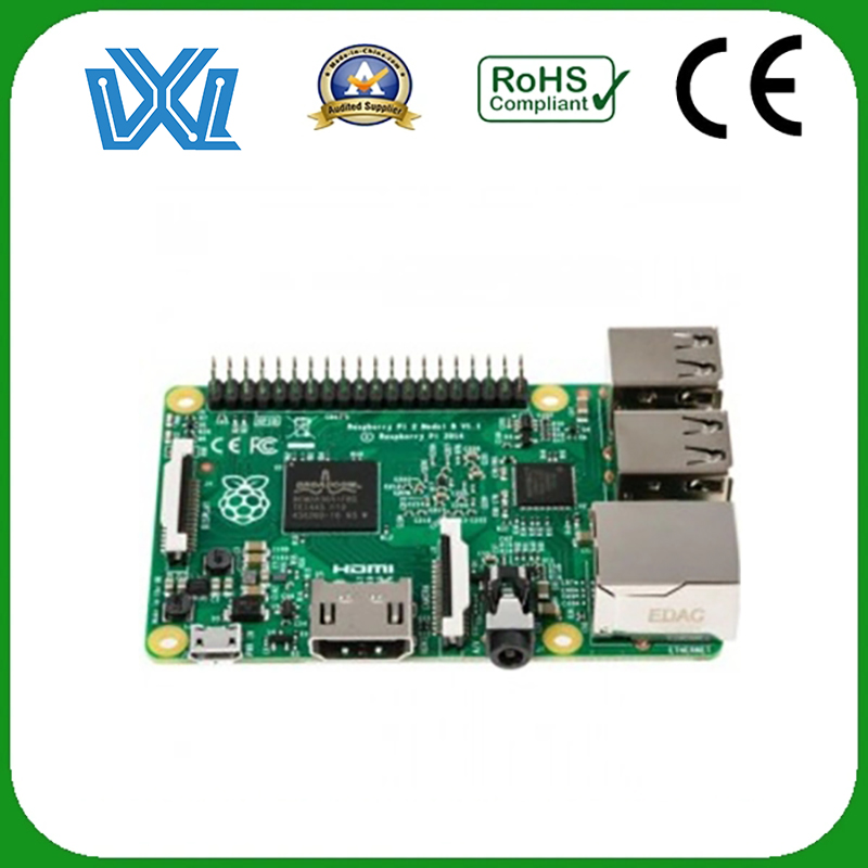
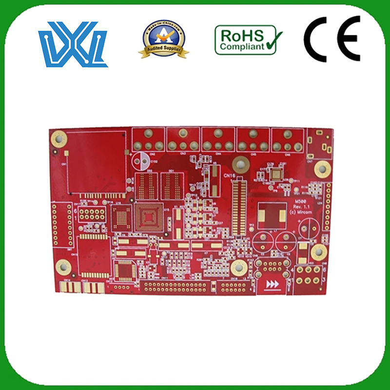
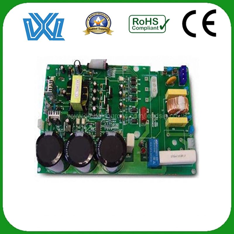
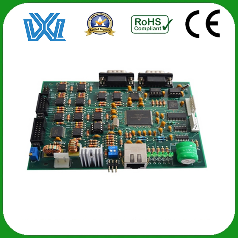
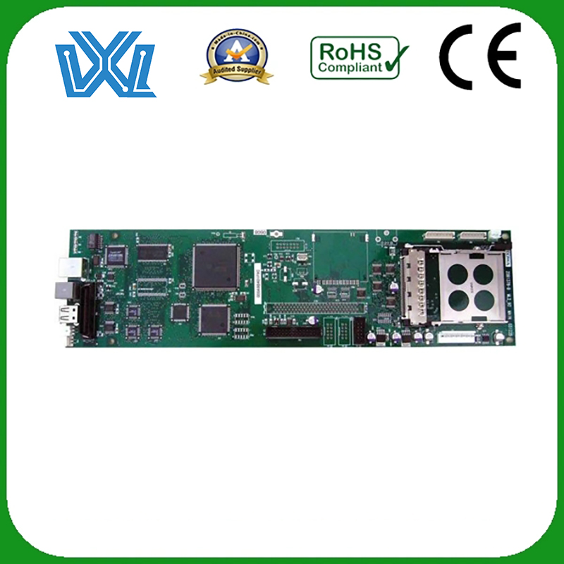
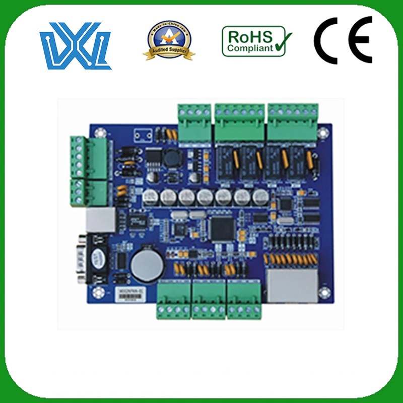
Product detail pictures:


Related Product Guide:
Just about every member from our large efficiency income crew values customers' wants and enterprise communication for OEM Mcpcb Manufacturers - Customized PCB Assembly and PCBA – Weilian Electronics , The product will supply to all over the world, such as: Luxemburg, azerbaijan, Canada, With all these supports, we can serve every customer with quality product and timely shipping with highly responsibility. Being a young growing company, we might not the best, but we are trying our best to be your good partner.
This company has a lot of ready-made options to choose and also could custom new program according to our demand, which is very nice to meet our needs.
Products categories
-
OEM Pcb On Pcb Manufacturer - PCB Assembly for...
-
Custom Printed Circuit Board Design Manufacture...
-
ODM Populated Circuit Board Factory - PCB Asse...
-
ODM Pcb Material Manufacturer - PCB Assembly f...
-
OEM Pcb Layout Design Factories - One-Stop OEM...
-
ODM Pcb Board Components Supplier - PCBA and P...


