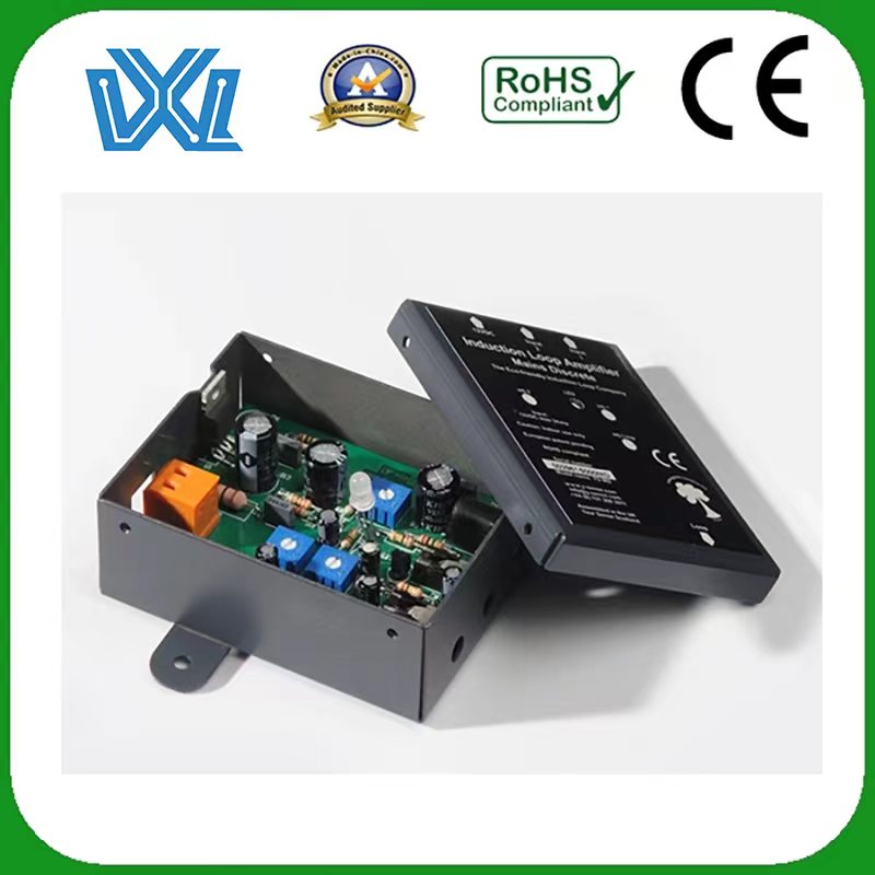
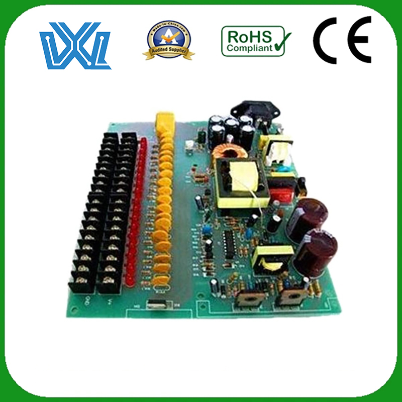
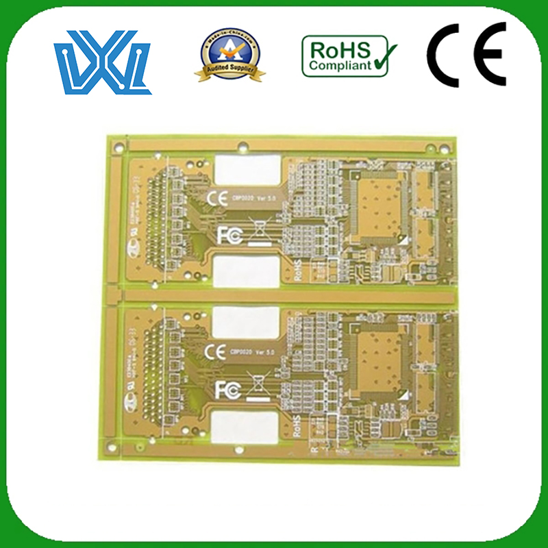
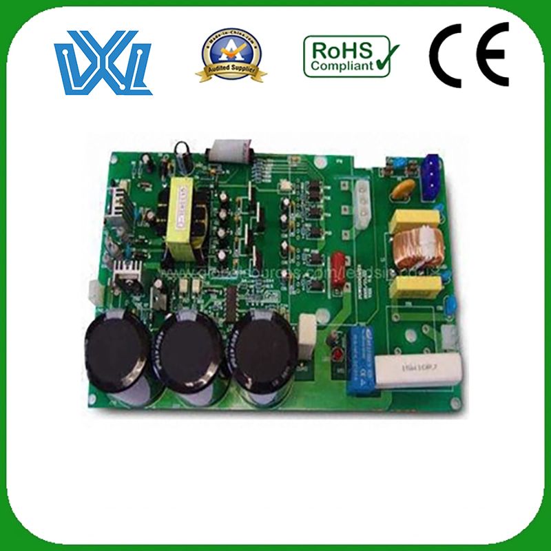
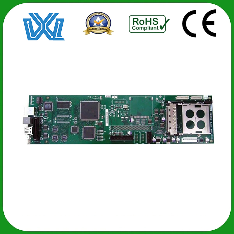
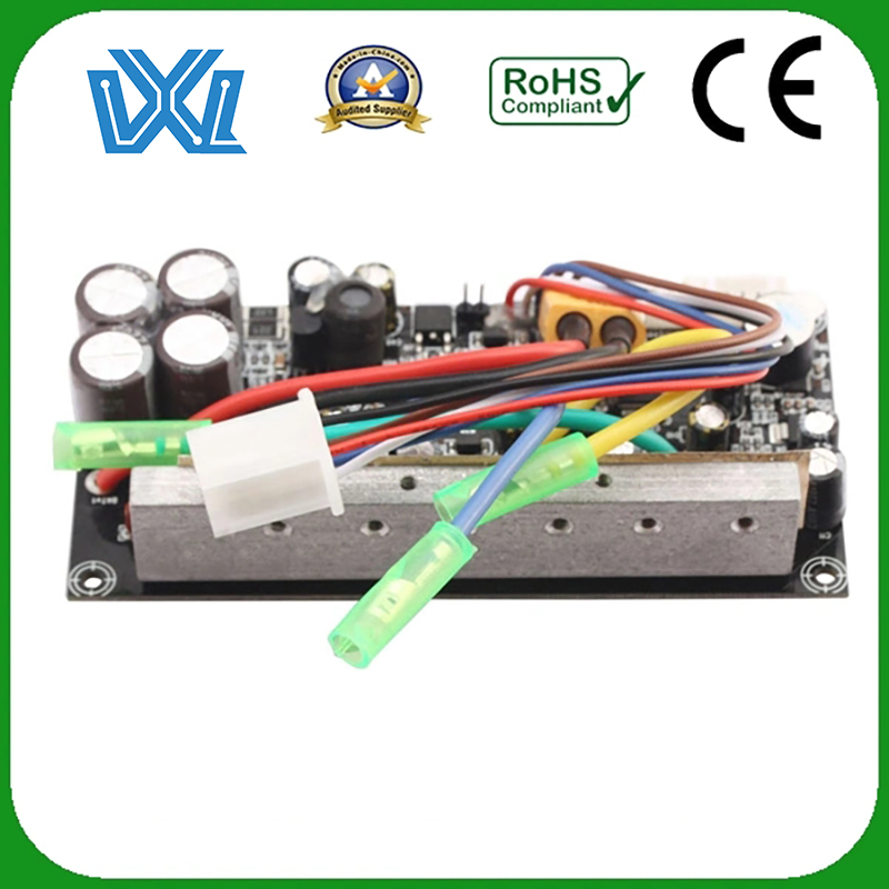
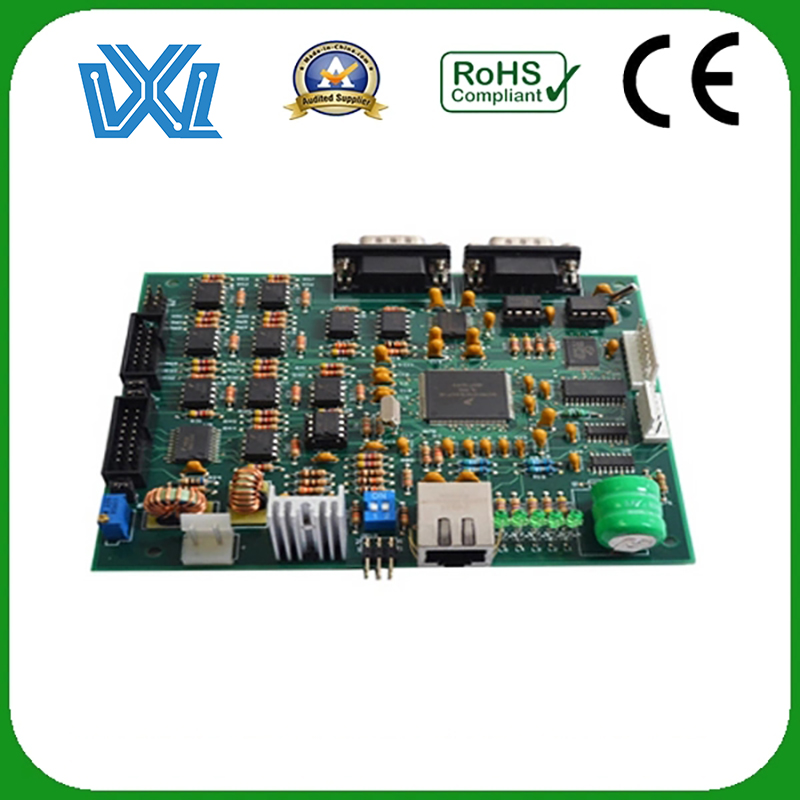
Double Side Rigid SMT PCB Assembly Circuit Board


Product Details
| Quote&Production Requirement | Gerber File or PCB File for Bare PCB Board Fabrication |
| Bom(Bill of Material) for Assembly,PNP(Pick and Place file) and Components Position also needed in assembly | |
| To reduce the quote time, please provide us the full part number for each components,Quantity per board also the quantity for orders. | |
| Testing Guide&Function Testing method to ensure the quality to reach nearly 0% scrap rate | |
| OEM/ODM/EMS Services | PCBA, PCB assembly: SMT & PTH & BGA |
| PCBA and enclosure design | |
| Components sourcing and purchasing | |
| Quick prototyping | |
| Plastic injection molding | |
| Metal sheet stamping | |
| Final assembly | |
| Test: AOI, In-Circuit Test (ICT), Functional Test (FCT) | |
| Custom clearance for material importing and product exporting |
Our Process
1. Immersion gold process: The purpose of the immersion gold process is to deposit a nickel-gold coating with stable color, good brightness, smooth coating and good solderability on the surface of the PCB, which can be basically divided into four stages: pretreatment ( Degreasing, micro-etching, activation, post-dipping), immersion nickel, immersion gold, post-treatment, (waste gold washing, DI washing, drying).
2. Lead-sprayed tin: The lead-containing eutectic temperature is lower than that of the lead-free alloy. The specific amount depends on the composition of the lead-free alloy. For example, the eutectic of SNAGCU is 217 degrees. The soldering temperature is the eutectic temperature plus 30-50 degrees, depending on the composition. Actual adjustment, the leaded eutectic is 183 degrees. Mechanical strength, brightness, etc. lead are better than lead-free.
3. Lead-free tin spraying: Lead will improve the activity of the tin wire in the welding process. The lead tin wire is easier to use than the lead-free tin wire, but the lead is poisonous, and it is not good for the human body if it is used for a long time. And lead-free tin will have a higher melting point than lead-tin, so that the solder joints are much stronger.
The specific process of PCB double-sided circuit board production process
1. CNC drilling
In order to increase the assembly density, the holes on the double-sided circuit board of the PCB are getting smaller and smaller. Generally, double-sided pcb boards are drilled with CNC drilling machines to ensure accuracy.
2. Electroplating hole process
The plated hole process, also known as metallized hole, is a process in which the entire hole wall is plated with metal so that the conductive patterns between the inner and outer layers of a double-sided printed circuit board can be electrically interconnected.
3. Screen printing
Special printing materials are used for screen printing circuit patterns, solder mask patterns, character mark patterns, etc.
4. Electroplating tin-lead alloy
Electroplating tin-lead alloys has two functions: first, as an anti-corrosion protective layer during electroplating and etching; second, as a solderable coating for the finished board. Electroplating tin-lead alloys must strictly control the bath and process conditions. The thickness of the tin-lead alloy plating layer should be more than 8 microns, and the hole wall should not be less than 2.5 microns.
printed circuit board
5. Etching
When using a tin-lead alloy as a resist layer to fabricate a double-sided panel by a patterned electroplating etching method, an acid copper chloride etching solution and a ferric chloride etching solution cannot be used because they also corrode the tin-lead alloy. In the etching process, “side etching” and coating broadening are factors that affect the etching: quality
(1) Side corrosion. Side corrosion is the phenomenon of sinking or sinking of conductor edges caused by etching. The extent of side corrosion is related to etching solution, equipment and process conditions. The less flank corrosion the better.
(2) The coating is widened. The widening of the coating is due to the thickening of the coating, which makes the width of one side of the wire exceed the width of the finished bottom plate.
6. Gold plating
Gold plating has excellent electrical conductivity, small and stable contact resistance and excellent wear resistance, and is the best plating material for printed circuit board plugs. At the same time, it has excellent chemical stability and solderability, and can also be used as a corrosion-resistant, solderable and protective coating on surface mount PCBs.
7. Hot melt and hot air leveling
(1) Hot melt. The pcb coated with Sn-Pb alloy is heated to above the melting point of Sn-Pb alloy, so that Sn-Pb and Cu form a metal compound, so that the Sn-Pb coating is dense, bright and pinhole-free, and the corrosion resistance and solderability of the coating are improved. sex. Hot-melt commonly used glycerol hot-melt and infrared hot-melt.
(2) Hot air leveling. Also known as tin spraying, the solder mask-coated printed circuit board is leveled with flux by hot air, then invades the molten solder pool, and then passes between two air knives to blow off the excess solder to get a bright , uniform, smooth solder coating. Generally, the temperature of the solder bath is controlled at 230~235, the temperature of the air knife is controlled at above 176, the dip welding time is 5~8s, and the coating thickness is controlled at 6~10 microns.
Double Sided Printed Circuit Board
If the PCB double-sided circuit board is scrapped, it cannot be recycled, and its manufacturing quality will directly affect the quality and cost of the final product.
Factory Show