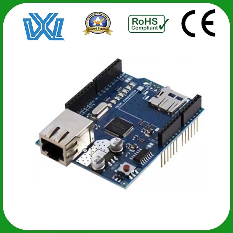
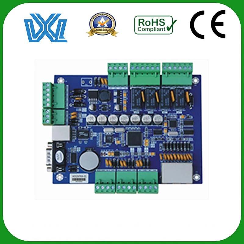
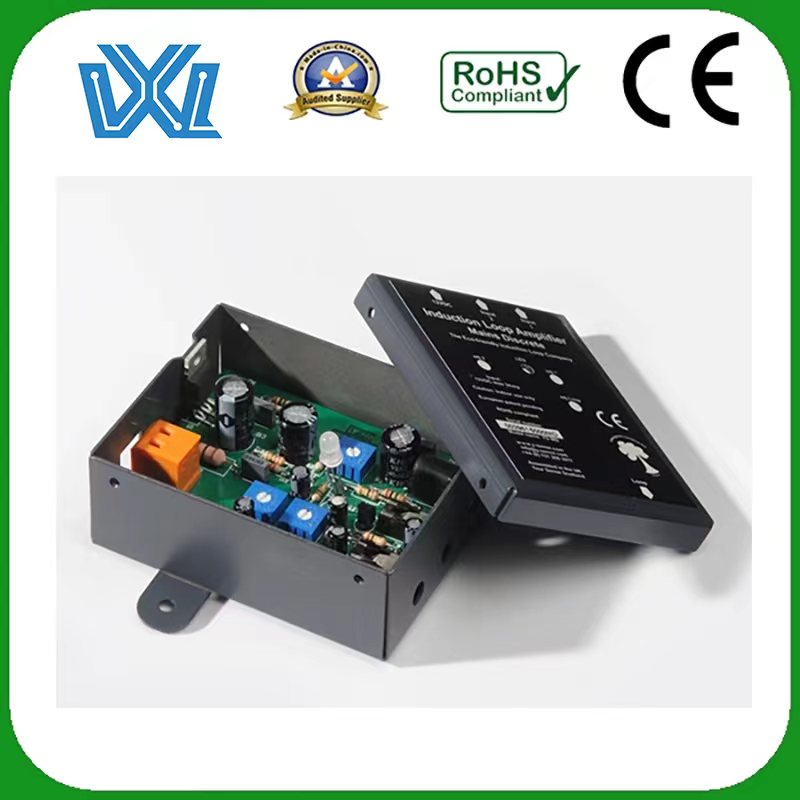
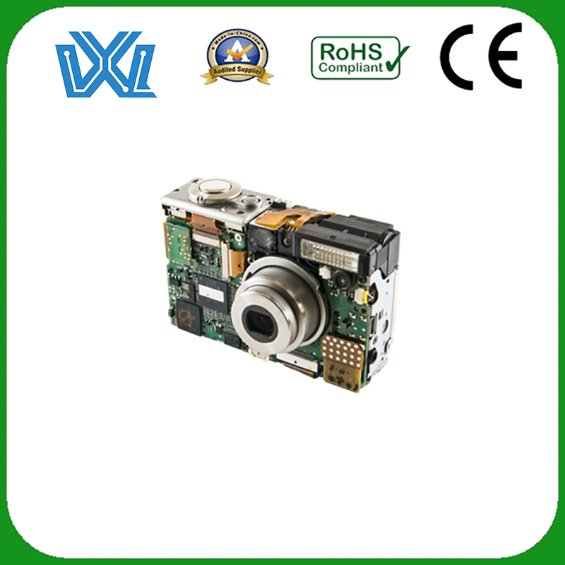
High Quality Printed Circuit Board PCB


PCB (PCB Assembly) Process Capability
| Technical Requirement | Professional Surface-mounting and Through-hole soldering Technology |
| Various sizes like 1206,0805,0603 components SMT technology | |
| ICT(In Circuit Test),FCT(Functional Circuit Test) technology | |
| PCB Assembly With UL,CE,FCC,Rohs Approval | |
| Nitrogen gas reflow soldering technology for SMT | |
| High Standard SMT&Solder Assembly Line | |
| High density interconnected board placement technology capacity | |
| Quote&Production Requirement | Gerber File or PCB File for Bare PCB Board Fabrication |
| Bom(Bill of Material) for Assembly,PNP(Pick and Place file) and Components Position also needed in assembly | |
| To reduce the quote time, please provide us the full part number for each components,Quantity per board also the quantity for orders. | |
| Testing Guide&Function Testing method to ensure the quality to reach nearly 0% scrap rate |
About
PCB have developed from single-layer to double-sided, multi-layer and flexible boards, and are constantly developing in the direction of high precision, high density and high reliability. Continuously shrinking the size, reducing the cost, and improving the performance will make the printed circuit board still maintain a strong vitality in the development of electronic products in the future. In the future, the development trend of printed circuit board manufacturing technology is to develop in the direction of high density, high precision, small aperture, thin wire, small pitch, high reliability, multi-layer, high-speed transmission, light weight and thin shape.
Detailed steps and precautions of PCB production
1. Design
Before the manufacturing process begins, the PCB needs to be designed/layout by a CAD operator based on a working circuit schematic. Once the design process is complete, a set of documents is provided to the PCB manufacturer. Gerber files are included in the documentation, which includes layer-by-layer configuration, drillthrough files, pick and place data, and text annotations. Processing prints, providing processing instructions critical to manufacturing, all PCB specifications, dimensions and tolerances.
2. Preparation before manufacturing
Once the PCB house receives the designer’s file package, they can begin creating the manufacturing process plan and artwork package. Manufacturing specifications will determine the plan by listing things like material type, surface finish, plating, array of work panels, process routing, and more. In addition, a set of physical artworks can be created through a film plotter. Artwork will include all layers of the PCB as well as artwork for soldermask and term marking.
3. Material preparation
The PCB specification required by the designer determines the material type, core thickness and copper weight used to start the material preparation. Single-sided and double-sided rigid PCBs do not require any inner layer processing and go directly to the drilling process. If the PCB is multi-layered, a similar material preparation will be done, but in the form of inner layers, which are usually much thinner and can be built up to a predetermined final thickness (stackup).
A common production panel size is 18″x24″, but any size can be used as long as it is within the PCB manufacturing capabilities.
4. Multilayer PCB only – inner layer processing
After the proper dimensions, material type, core thickness and copper weight of the inner layer are prepared, it is sent to drill the machined holes and then print. Both sides of these layers are coated with photoresist. Align the sides using inner layer artwork and tool holes, then expose each side to UV light detailing an optical negative of the traces and features specified for that layer. UV light falling on the photoresist bonds the chemical to the copper surface, and the remaining unexposed chemical is removed in a developing bath.
The next step is to remove the exposed copper through an etching process. This leaves copper traces hidden under the photoresist layer. During the etching process, both the concentration of the etchant and the exposure time are key parameters. The resist is then stripped, leaving traces and features on the inner layer.
Most PCB suppliers use automated optical inspection systems to inspect layers and post-etch punches to optimize lamination tool holes.
5. Multilayer PCB only – Laminate
A predetermined stack of the process is established during the design process. The lamination process is carried out in a clean room environment with a complete inner layer, prepreg, copper foil, press plates, pins, stainless steel spacers and backing plates. Each press stack can accommodate 4 to 6 boards per press opening, depending on the thickness of the finished PCB. An example of a 4-layer board stackup would be: platen, steel separator, copper foil (4th layer), prepreg, core 3-2 layers, prepreg, copper foil, and repeat. After 4 to 6 PCBs are assembled, secure a top platen and place it in the lamination press. The press ramps up to the contours and applies pressure until the resin melts, at which point the prepreg flows, bonding the layers together, and the press cools. When taken out and ready
6. Drilling
The drilling process is performed by a CNC-controlled multi-station drilling machine that uses a high RPM spindle and a carbide drill bit designed for PCB drilling. Typical vias can be as small as 0.006″ to 0.008″ drilled at speeds above 100K RPM.
The drilling process creates a clean, smooth hole wall that won’t damage the inner layers, but the drilling provides a pathway for interconnection of the inner layers after plating, and the non-through hole ends up being home to through-hole components.
Non-plated holes are usually drilled as a secondary operation.
7. Copper plating
Electroplating is widely used in PCB production where plated through holes are required. The goal is to deposit a layer of copper on a conductive substrate through a series of chemical treatments, and then through subsequent electroplating methods to increase the thickness of the copper layer to a specific design thickness, typically 1 mil or more.
8. Outer layer treatment
The outer layer processing is actually the same as the process previously described for the inner layer. Both sides of the top and bottom layers are coated with photoresist. Align the sides using outer artwork and tool holes, then expose each side to UV light to detail the optical negative pattern of traces and features. UV light falling on the photoresist bonds the chemical to the copper surface, and the remaining unexposed chemical is removed in a developing bath. The next step is to remove the exposed copper through an etching process. This leaves copper traces hidden under the photoresist layer. The resist is then stripped, leaving traces and features on the outer layer. Outer layer defects can be found before solder mask using automated optical inspection.
9. Solder paste
Solder mask application is similar to inner and outer layer processes. The main difference is the use of a photoimageable mask instead of photoresist over the entire surface of the production panel. Then use the artwork to take images on the top and bottom layers. After exposure, the mask is peeled off in the imaged area. The purpose is to expose only the area where the components will be placed and soldered. The mask also limits the surface finish of the PCB to the exposed areas.
10. Surface treatment
There are several options for the final surface finish. Gold, silver, OSP, lead-free solder, lead-containing solder, etc. All of these are valid, but really boil down to design requirements. Gold and silver are applied by electroplating, while lead-free and lead-containing solders are applied horizontally by hot air solder.
11. Nomenclature
Most PCBs are shielded on the markings on their surface. These markings are mainly used in the assembly process and include examples such as reference markings and polarity markings. Other markings can be as simple as part number identification or manufacturing date codes.
12. Sub-board
PCBs are produced in full production panels that need to be moved out of their manufacturing contours. Most PCBs are set up in arrays to improve assembly efficiency. There can be an infinite number of these arrays. Can’t describe.
Most arrays are either profile milled on a CNC mill using carbide tools or scored using diamond-coated serrated tools. Both methods are valid, and the choice of method is usually determined by the assembly team, which usually approves the array built at an early stage.
13. Test
PCB manufacturers typically use a flying probe or bed of nails testing process. Test method determined by product quantity and/or available equipment
One-stop Solution
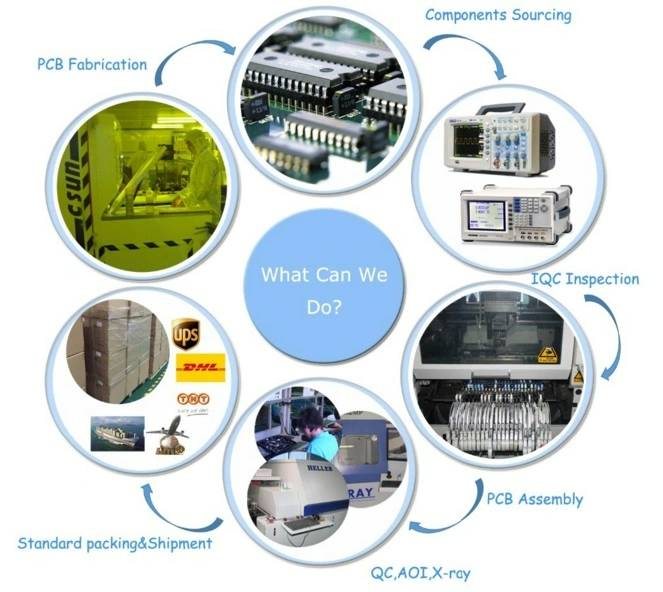
Factory Show

Our Service
1. PCB Assembly Services:SMT,DIP&THT,BGA repair and reballing
2. ICT, Constant Temperature Burn-in and Function Test
3. Stencil,Cables and Enclosure building
4. Standard Packing and On time Delivery