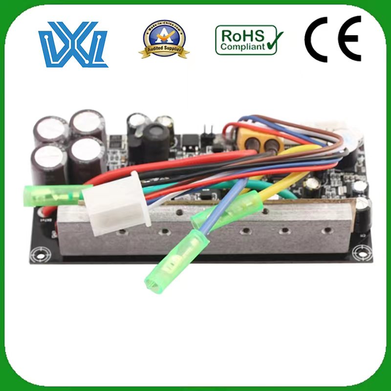
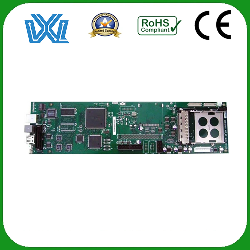
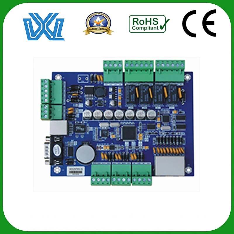
PCBA and PCB Board Assembly for Electronics Products


Product Details
| Model NO. | ETP-005 | Condition | New |
| Min Trace Width/Space | 0.075/0.075mm | Copper Thickness | 1 – 12 Oz |
| Assembly Modes | SMT, DIP, Through Hole | Application Field | LED, Medical, Industrial, Control Board |
| Samples Run | Available | Transport Package | Vacuum Packing/Blister/Plastic /Cartoon |
PCB (PCB Assembly) Process Capability
| Technical Requirement | Professional Surface-mounting and Through-hole soldering Technology |
| Various sizes like 1206,0805,0603 components SMT technology | |
| ICT(In Circuit Test),FCT(Functional Circuit Test) technology | |
| PCB Assembly With UL,CE,FCC,Rohs Approval | |
| Nitrogen gas reflow soldering technology for SMT | |
| High Standard SMT&Solder Assembly Line | |
| High density interconnected board placement technology capacity | |
| Quote&Production Requirement | Gerber File or PCB File for Bare PCB Board Fabrication |
| Bom(Bill of Material) for Assembly,PNP(Pick and Place file) and Components Position also needed in assembly | |
| To reduce the quote time, please provide us the full part number for each components,Quantity per board also the quantity for orders. | |
| Testing Guide&Function Testing method to ensure the quality to reach nearly 0% scrap rate |
The specific process of PCBA
1) Conventional double-sided process flow and technology.
① Material cutting—drilling—hole and full plate electroplating—pattern transfer (film formation, exposure, development)—etching and film removal—solder mask and characters—HAL or OSP, etc.—shape processing—inspection—finished product
② Cutting material—drilling—holeization—pattern transfer—electroplating—film stripping and etching—anti-corrosion film removal (Sn, or Sn/pb)—plating plug- –Solder mask and characters—HAL or OSP, etc.—shape processing—inspection—finished product
(2) Conventional multi-layer board process and technology.
Material cutting—inner layer production—oxidation treatment—lamination—drilling—hole plating (can be divided into full board and pattern plating)—outer layer production—surface coating —Shape processing—Inspection—Finished product
(Note 1): The inner layer production refers to the process of the in-process board after the material is cut—pattern transfer (film formation, exposure, development)—etching and film removal—inspection, etc.
(Note 2): Outer layer fabrication refers to the process of plate-making via hole electroplating—pattern transfer (film formation, exposure, development)—etching and film stripping.
(Note 3): Surface coating (plating) means that after the outer layer is made—solder mask and characters—coating (plating) layer (such as HAL, OSP, chemical Ni/Au, chemical Ag, chemical Sn, etc. Wait).
(3) Buried/blind via multilayer board process flow and technology.
Sequential lamination methods are generally used. which is:
Material cutting—forming core board (equivalent to conventional double-sided or multi-layer board)—lamination—the following process is the same as conventional multi-layer board.
(Note 1): Forming the core board refers to the formation of a multi-layer board with buried/blind holes according to the structural requirements after the double-sided or multi-layer board is formed by conventional methods. If the aspect ratio of the hole of the core board is large, the hole blocking treatment should be carried out to ensure its reliability.
(4) The process flow and technology of the laminated multi-layer board.
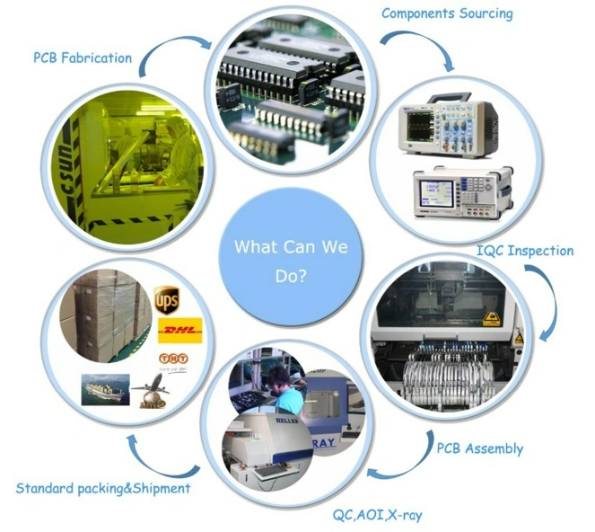
One-stop Solution
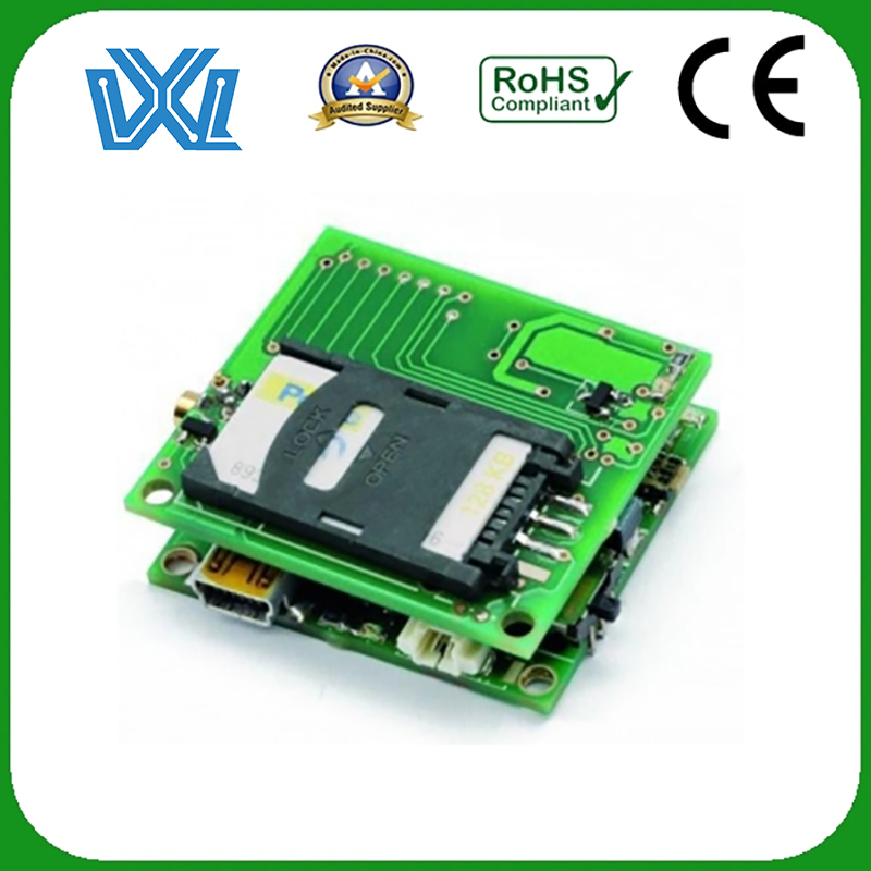
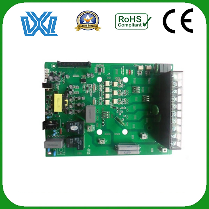
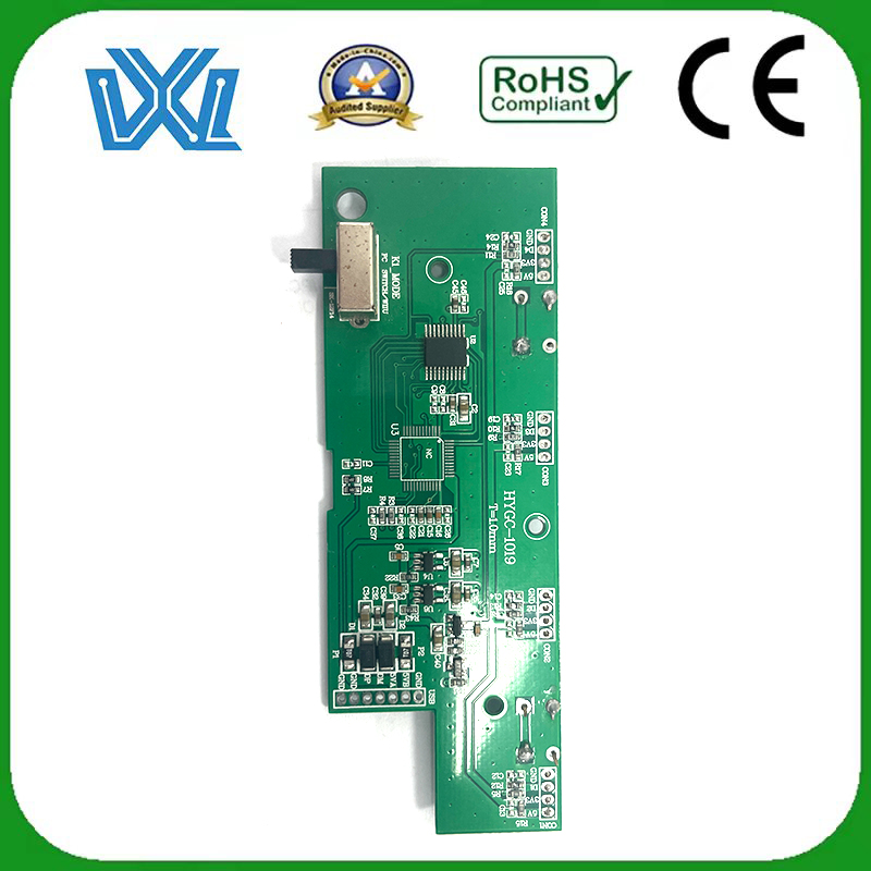
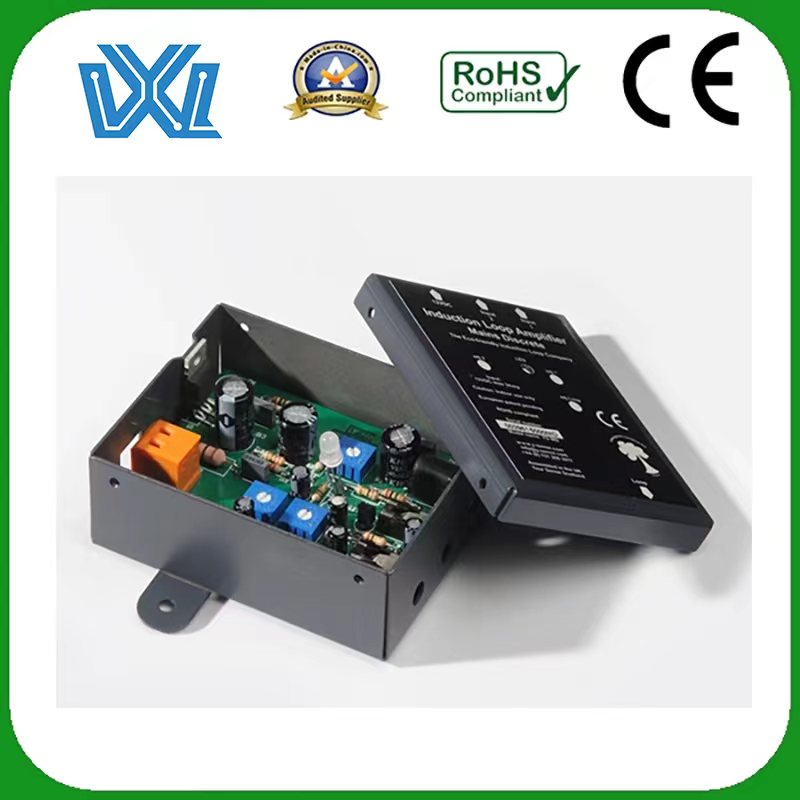
Shop Exhibition

As a service-leading PCB manufacturing and PCB assembly (PCBA) partner, Evertop strives to support international small-medium business with engineering experience in Electronic Manufacturing Services (EMS) for years.