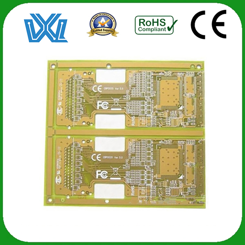
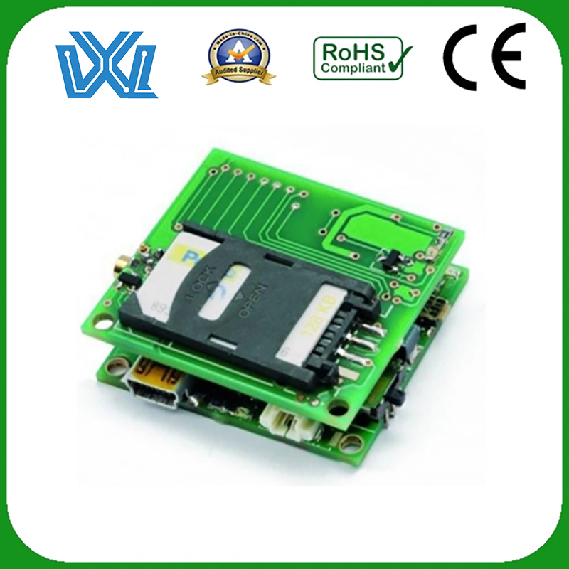
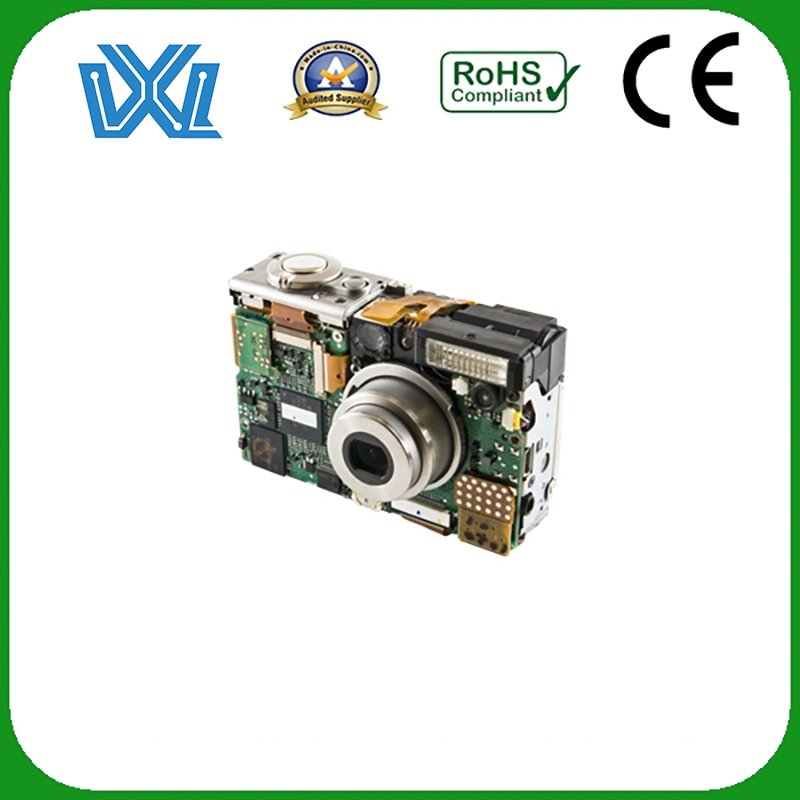
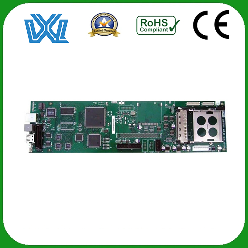
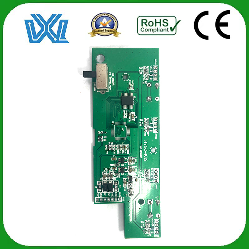
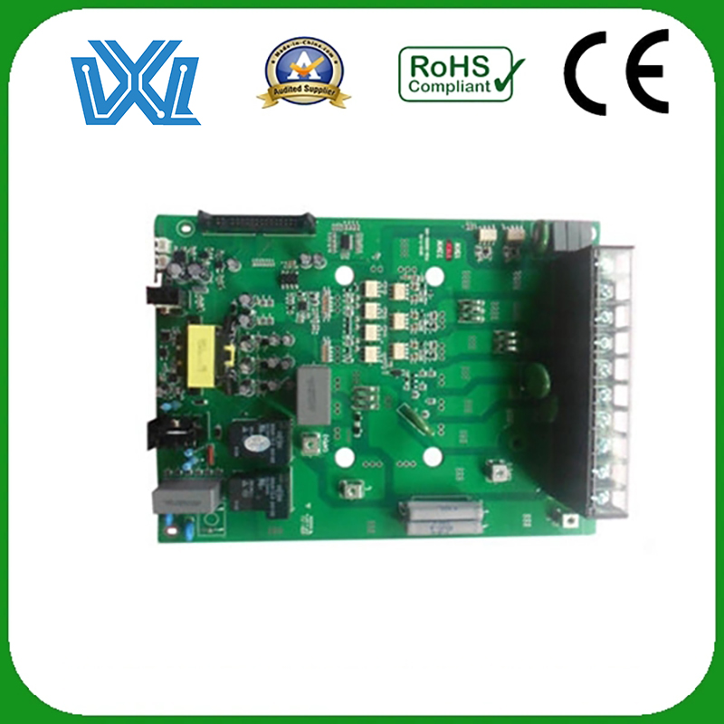
Immersion Gold Multilayer PCB Printed Circuit Board with SMT and DIP
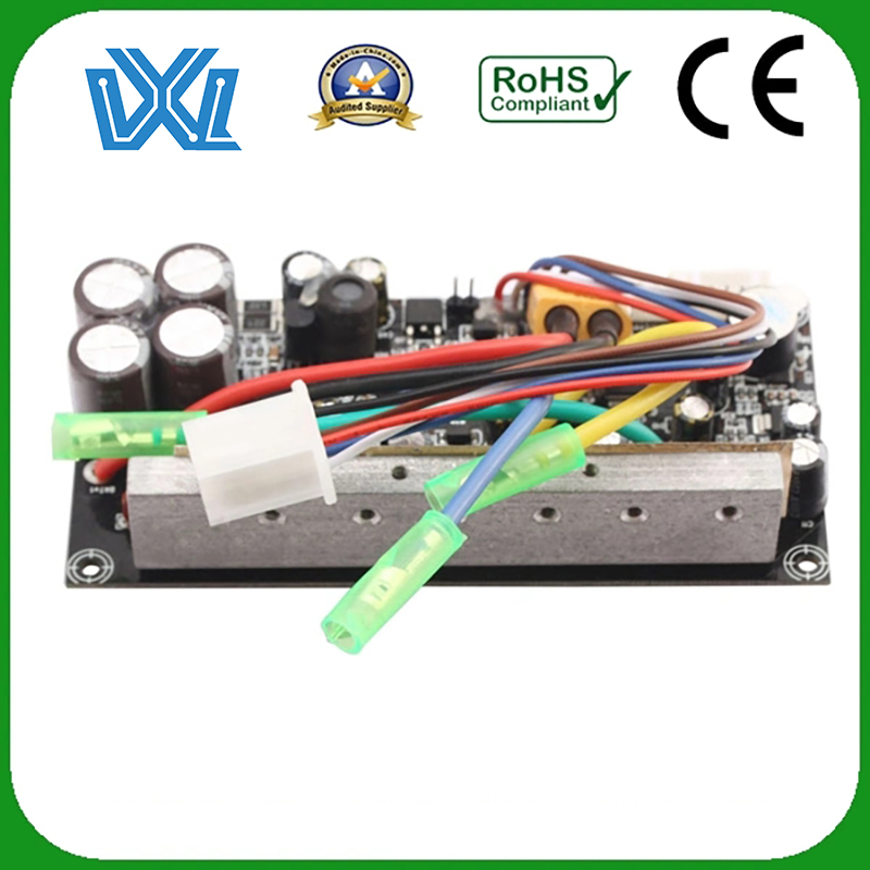


Product Details
| Product Type | PCB Assembly | Min.Hole Size | 0.12mm |
| Solder Mask Colour | Green, Blue, White, Black, Yellow, Red etc Surface Finish |
Surface Finish | HASL, Enig, OSP, Gold Finger |
| Min Trace Width/Space | 0.075/0.075mm | Copper Thickness | 1 – 12 Oz |
| Assembly Modes | SMT, DIP, Through Hole | Application Field | LED, Medical, Industrial, Control Board |
| Samples Run | Available | Transport Package | Vacuum Packing/Blister/Plastic /Cartoon |
More Related Information
| OEM/ODM/EMS Services | PCBA, PCB assembly: SMT & PTH & BGA |
| PCBA and enclosure design | |
| Components sourcing and purchasing | |
| Quick prototyping | |
| Plastic injection molding | |
| Metal sheet stamping | |
| Final assembly | |
| Test: AOI, In-Circuit Test (ICT), Functional Test (FCT) | |
| Custom clearance for material importing and product exporting | |
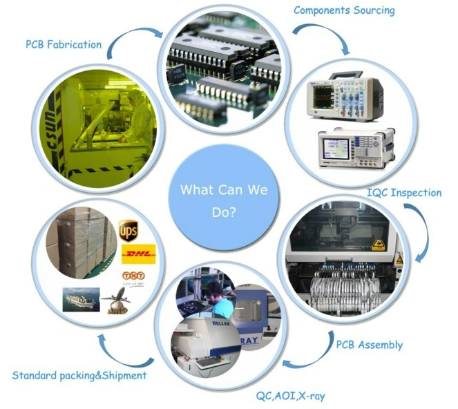
| Other PCB Assembly Equipments | SMT Machine: SIEMENS SIPLACE D1/D2 / SIEMENS SIPLACE S20/F4 |
| Reflow Oven: FolunGwin FL-RX860 | |
| Wave Soldering Machine: FolunGwin ADS300 | |
| Automated Optical Inspection (AOI): Aleader ALD-H-350B,X-RAY Testing Service | |
| Fully Automatic SMT Stencil Printer: FolunGwin Win-5 |
1. SMT is one of the basic components of electronic components. It is called surface mount technology (or surface mount technology). It is divided into no leads or short leads. It is a circuit assembly that is assembled by reflow soldering or dip soldering. Technology is also the most popular technology and process in the electronic assembly industry.
Features: Our substrates can be used for power supply, signal transmission, heat dissipation, and structure provision.
Features: Can withstand the temperature and time of curing and soldering.
The flatness meets the requirements of the manufacturing process.
Suitable for rework work.
Suitable for the manufacturing process of the substrate.
Low dielectric count and high resistance.
The commonly used materials for our product substrates are healthy and environmentally friendly epoxy resins and phenolic resins, which have good flame-retardant properties, temperature properties, mechanical and dielectric properties, and low cost.
The above mentioned is that the rigid substrate is solid state.
Our products also have flexible substrates, which can be used to save space, fold or turn, move, and are made of very thin insulating sheets with good high frequency performance.
The disadvantage is that the assembly process is difficult, and it is not suitable for micro-pitch applications.
I think the characteristics of the substrate are small leads and spacing, large thickness and area, better thermal conductivity, tougher mechanical properties, and better stability. I think the placement technology on the substrate is electrical performance, there are reliability, standard parts.
We not only have fully automatic and integrated operation, but also have the double guarantee of manual audit and machine audit, and the pass rate of products is as high as 99.98%.
2. PCB is the most important electronic components, and there is no one. Usually, a conductive pattern made of printed circuits, printed components or a combination of the two on the insulating material according to a predetermined design is called a printed circuit. The conductive pattern that provides electrical connection between components on the insulating substrate is called a printed circuit board (or printed circuit board), which is an important support for electronic components and a carrier that can carry components.
I think we usually open the computer keyboard to see a soft film (flexible insulating substrate) printed with silver-white (silver paste) conductive graphics and positioning graphics. Because this kind of pattern is obtained by the general screen printing method, we call this printed circuit board flexible silver paste printed circuit board. The printed circuit boards on various computer motherboards, graphics cards, network cards, modems, sound cards and household appliances that we see in the computer city are different.
The base material it uses is made of paper base (usually used for single side) or glass cloth base (usually used for double-sided and multi-layer), pre-impregnated phenolic or epoxy resin, one side or both sides of the surface is pasted with copper cladding and then laminated and cured made. This kind of circuit board copper-clad sheet, we call it a rigid board. After making a printed circuit board, we call it a rigid printed circuit board.
A printed circuit board with a printed circuit pattern on one side is called a single-sided printed circuit board, a printed circuit board with a printed circuit pattern on both sides, and a printed circuit board formed by double-sided interconnection through the metallization of the holes, we call it a double-sided board. If a printed circuit board with double-sided inner layer, two single-sided outer layer, or two double-sided inner layer and two single-sided outer layer is used, the positioning system and insulating bonding material are alternated together and The printed circuit board with the conductive pattern interconnected according to the design requirements becomes a four-layer and six-layer printed circuit board, also known as a multi-layer printed circuit board.
3. PCBA is one of the basic components of electronic components. The PCB goes through the entire process of surface mount technology (SMT) and the insertion of DIP plug-ins, which is called the PCBA process. In fact, it is a PCB with a piece attached. One is the finished board and the other is the bare board.
PCBA can be understood as a finished circuit board, that is, after all the processes of the circuit board are completed, PCBA can be counted. Due to the continuous miniaturization and refinement of electronic products, most of the current circuit boards are attached with etching resists (lamination or coating). After exposure and development, circuit boards are made by etching.
In the past, the understanding of cleaning was not enough because the assembly density of PCBA was not high, and it was also believed that the flux residue was non-conductive and benign, and would not affect electrical performance.
Today’s electronic assemblies tend to be miniaturized, even smaller devices, or smaller pitches. The pins and the pads are getting closer and closer. Today’s gaps are getting smaller and smaller, and contaminants may also get stuck in the gaps, which means that relatively small particles, if they remain between the two gaps, may also be Bad phenomenon caused by short circuit.
In recent years, the electronic assembly industry has become increasingly aware and vocal about cleaning, not only for product requirements, but also for environmental requirements and protection of human health. Therefore, there are many suppliers of cleaning equipment and solutions, and cleaning has also become one of the main contents of technical exchanges and discussions in the electronic assembly industry.
4. DIP is one of the basic components of electronic components. It is called dual in-line packaging technology, which refers to integrated circuit chips that are packaged in dual in-line packaging. This packaging form is also used in most small and medium-sized integrated circuits. , the number of pins generally does not exceed 100.
The CPU chip of DIP packaging technology has two rows of pins, which need to be inserted into the chip socket with DIP structure.
Of course, it can also be directly inserted into a circuit board with the same number of solder holes and geometric arrangement for soldering.
DIP packaging technology should take special care when inserting and unplugging from the chip socket to avoid damage to the pins.
Features are: multi-layer ceramic DIP DIP, single-layer ceramic DIP DIP, lead frame DIP (including glass ceramic sealing type, plastic packaging structure type, ceramic low melting glass packaging type) and so on.
DIP plug-in is a link in the electronic manufacturing process, there are manual plug-ins, but also AI machine plug-ins. Insert the specified material into the specified position. Manual plug-ins also have to go through wave soldering to solder electronic components on the board. For the inserted components, it is necessary to check whether they are inserted incorrectly or missed.
DIP plug-in post-soldering is a very important process in the processing of pcba patch, and its processing quality directly affects the function of pcba board, its importance is very important. Then post-soldering, because some components, according to the limitations of the process and materials, cannot be soldered by a wave soldering machine, and can only be done by hand.
This also reflects the importance of DIP plug-ins in electronic components. Only by paying attention to details can it be completely indistinguishable.
In these four major electronic components, each has its own advantages, but they complement each other to form this series of production processes. Only by checking the quality of the production products can a wide range of users and customers realize our intentions.
One-stop Solution
Factory Exhibition

As a service-leading PCB manufacturing and PCB assembly (PCBA) partner, Evertop strives to support international small-medium business with engineering experience in Electronic Manufacturing Services (EMS) for years.
FAQ
Q1: How do you make sure the quality of the PCBs?
A1: Our PCBs are all 100% test including Flying Probe Test, E-test or AOI.
Q2: Can I get the best price?
A2: Yes. To help customers control cost is what we are always trying to do. Our engineers will provide the best design to save PCB material.
Q3: Can I get a free sample?
A3: Yes, Welcome to experience our service and quality.You need make the payment at first, and we will return the sample cost when your next bulk order.