What are the PCB appearance inspection standards?
1. Packaging: colorless air bag vacuum packaging, with desiccant inside, tightly packed
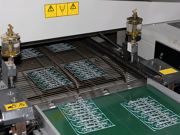
2. Silk screen printing: The silk screen printing of the characters and symbols on the surface of the PCB must be clear and obvious, and the color must comply with the regulations, without repeated printing, missing printing, multiple printing, position deviation, and misprinting.
3. Board edge board surface: Check whether there are stains, sundries, pits, tin slag residues on the PCB surface; whether the board surface is scratched and exposed to the substrate; There are layers, etc.
4. Conductors: No short circuit, open circuit, exposed copper in the conductor, floating copper foil, supplementary wiring, etc. Pads: The pads should be evenly tinned, and copper should not be exposed, damaged, peeled off, deformed, etc. Gold finger: luster, bumps/bubbles, stains, copper foil floating, surface coating, burrs, plating adhesion, etc.
5. Holes: Check against the previous batch of good PCBs to check whether there are missing drill holes, multiple drill holes, blocked holes, and hole deviation. Solder mask: You can use board washing water to wipe it during inspection to check its adhesion, check whether it will fall off, whether there are bubbles, whether there is any repair phenomenon, etc. The color of the solder mask must meet the regulations.
6. Marking: character, reference point, model version, fire rating/UL. standard, electrical test chapter, manufacturer’s nameplate, production date, etc.
7. Size measurement: measure whether the actual size of the incoming PCB is as specified in the order.
Warpage or curvature inspection:
8. Solderability test: Take part of the PCB for actual soldering, and check whether the parts can be easily soldered.
Post time: Apr-12-2023