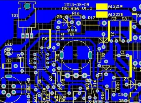
PCB layout rules:
1. Under normal circumstances, all components should be arranged on the same surface of the circuit board. Only when the top layer components are too dense can some devices with limited height and low heat generation, such as chip resistors, chip capacitors, and Chip ICs are placed on the bottom layer.
2. Under the premise of ensuring the electrical performance, the components should be placed on the grid and arranged parallel to each other or vertically in order to be neat and beautiful. In general, components are not allowed to overlap; the components should be arranged compactly, and the components should be arranged on the entire layout. Uniform distribution and consistent density.
3. The minimum spacing between adjacent pad patterns of different components on the circuit board should be above 1MM.
4. The distance from the edge of the circuit board is generally not less than 2MM. The best shape of the circuit board is a rectangle with an aspect ratio of 3:2 or 4:3. When the size of the circuit board is greater than 200MM by 150MM, the circuit board can bear Mechanical strength.
PCB Design Considerations
(1) Avoid arranging important signal lines on the edge of the PCB, such as clock and reset signals.
(2) The distance between the chassis ground wire and the signal line is at least 4 mm; keep the aspect ratio of the chassis ground wire less than 5:1 to reduce the inductance effect.
(3) Use the LOCK function to lock the devices and lines whose positions have been determined, so that they will not be misoperated in the future.
(4) The minimum width of the wire should not be less than 0.2mm (8mil). In high-density and high-precision printed circuits, the width and spacing of the wires are generally 12mil.
(5) The 10-10 and 12-12 principles can be applied to the wiring between the IC pins of the DIP package, that is, when two wires pass between the two pins, the pad diameter can be set to 50mil, and the line width and line spacing are both 10mil, when only one wire passes between the two pins, the pad diameter can be set to 64mil, and the line width and line spacing are both 12mil.
(6) When the diameter of the pad is 1.5mm, in order to increase the peeling strength of the pad, you can use a long circular pad with a length of not less than 1.5mm and a width of 1.5mm.
(7) Design When the traces connected to the pads are thin, the connection between the pads and the traces should be designed in a drop shape, so that the pads are not easy to peel and the traces and pads are not easy to disconnect.
(8) When designing large-area copper cladding, there should be windows on the copper cladding, heat dissipation holes should be added, and the windows should be designed into a mesh shape.
(9) Shorten the connection between high-frequency components as much as possible to reduce their distribution parameters and mutual electromagnetic interference. Components that are susceptible to interference cannot be too close to each other, and input and output components should be kept as far away as possible.
Post time: Apr-14-2023

