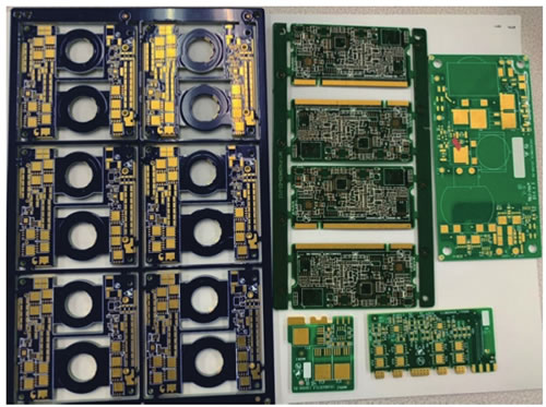
PCB is made by electronic printing technology, so it is called printed circuit board. Almost every kind of electronic equipment, ranging from earphones, batteries, calculators, to computers, communication equipment, airplanes, satellites, as long as electronic components such as integrated circuits are used, PCBs are used for the electrical interconnection between them.
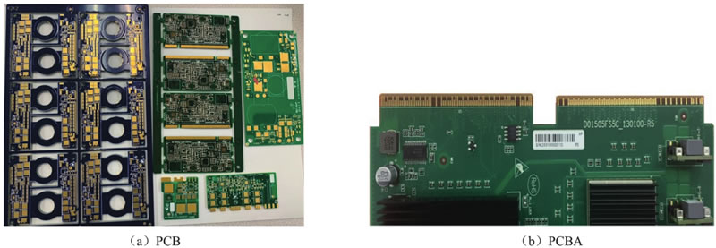
PCB and PCBA are PCBs with unmounted components, PCBA (Printed Circuit Board Assembly), that is, PCBs equipped with electronic components (such as chips, connectors, resistors, capacitors, inductors, etc.).
The origin of PCB
In 1925, Charles Ducas in the United States (the originator of the additive method) printed a circuit pattern on an insulating substrate, and then successfully made a conductor as a wiring by electroplating.
In 1936, the Austrian Paul Eisler (the originator of the subtractive method) was the first to use printed circuit boards in radios.
In 1943, Americans applied the technology to military radios. In 1948, the United States officially recognized the invention for commercial use.
Printed circuit boards have only been widely used since the mid-1950s, and today they dominate the electronics industry.
Printed circuit boards have developed from single-layer to double-sided, multi-layer and flexible, and still maintain their own development trends. Due to the continuous development in the direction of high precision, high density and high reliability, continuous reduction in size, cost reduction and performance improvement, printed circuit boards still maintain strong vitality in the development of future electronic equipment.
Discussions on the future development trend of printed circuit board manufacturing technology at home and abroad are basically consistent, that is, to high density, high precision, fine aperture, thin wire, small pitch, high reliability, multi-layer, high-speed transmission, light weight In terms of production, it is developing in the direction of increasing productivity, reducing costs, reducing pollution, and adapting to multi-variety and small-batch production.
The role of PCB
Before the printed circuit board appeared, the interconnection between electronic components was directly connected by wires to form a complete circuit.
After electronic equipment adopts printed circuit boards, due to the consistency of similar printed circuit boards, errors in manual wiring are avoided.
The printed circuit board can provide mechanical support for fixing and assembling various electronic components such as integrated circuits, complete the wiring and electrical connection or electrical insulation between various electronic components such as integrated circuits, and provide the required electrical characteristics, such as characteristics Impedance, etc., can provide solder mask graphics for automatic soldering, and provide identification characters and graphics for component insertion, inspection, and maintenance.
Classification of PCB
1. Classification by purpose
Civilian printed circuit boards (consumer): printed circuit boards used in toys, cameras, televisions, audio equipment, mobile phones, etc.
Industrial printed circuit boards (equipment): printed circuit boards used in security, automobiles, computers, communication machines, instruments, etc.
Military printed circuit boards: printed circuit boards used in aerospace and radar, etc.
2. Classification by substrate type
Paper-based printed circuit boards: phenolic paper-based printed circuit boards, epoxy paper-based printed circuit boards, etc.
Glass cloth-based printed circuit boards: epoxy glass cloth-based printed circuit boards, PTFE glass cloth-based printed circuit boards, etc.
Synthetic fiber printed circuit board: epoxy synthetic fiber printed circuit board, etc.
Organic film substrate printed circuit board: nylon film printed circuit board, etc.
Ceramic substrate printed circuit boards.
Metal core based printed circuit boards.
3. Classification by structure
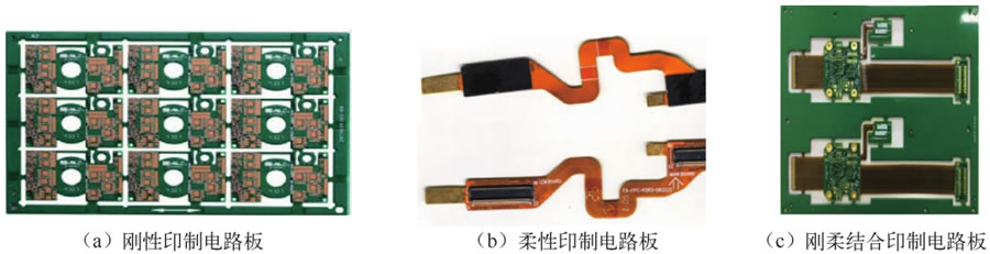
According to the structure, printed circuit boards can be divided into rigid printed circuit boards, flexible printed circuit boards and rigid-flexible printed circuit boards
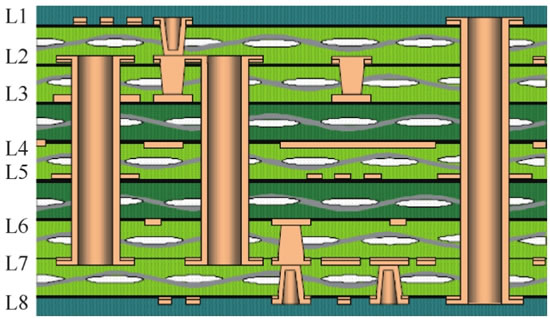
4. Classified according to the number of layers
According to the number of layers, printed circuit boards can be divided into single-sided boards, double-sided boards, multi-layer boards and HDI boards (high-density interconnect boards).
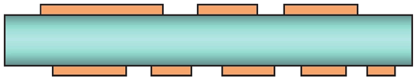
1) Single sided
A single-sided board refers to a circuit board that is wired on only one side (soldering side) of the circuit board, and all components, component labels and text labels are placed on the other side (component side).
The biggest feature of the single-sided panel is its low price and simple manufacturing process. However, since the wiring can only be carried out on one surface, the wiring is more difficult, and the wiring is prone to failure, so it is only suitable for some relatively simple circuits.

2) Double sided
The double-sided board is wired on both sides of the insulating board, one side is used as the top layer, and the other side is used as the bottom layer. The top and bottom layers are electrically connected through vias.
Usually, components on a two-layer board are placed on the top layer; however, sometimes components can be placed on both layers in order to reduce the size of the board. The double-layer board is characterized by moderate price and easy wiring. It is the most commonly used type in ordinary circuit boards.
3) Multi-layer board
Printed circuit boards with more than two layers are collectively referred to as multilayer boards.
4) HDI board
The HDI board is a circuit board with a relatively high circuit distribution density using micro-blind buried hole technology.
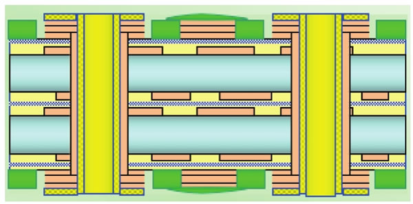
PCB structure
PCB is mainly composed of copper clad laminates (Copper Clad Laminates, CCL), prepreg (PP sheet), copper foil (Copper Foil), solder mask (also known as solder mask) (Solder Mask). At the same time, in order to protect the exposed copper foil on the surface and ensure the welding effect, it is also necessary to carry out surface treatment on the PCB, and sometimes it is also marked with characters.
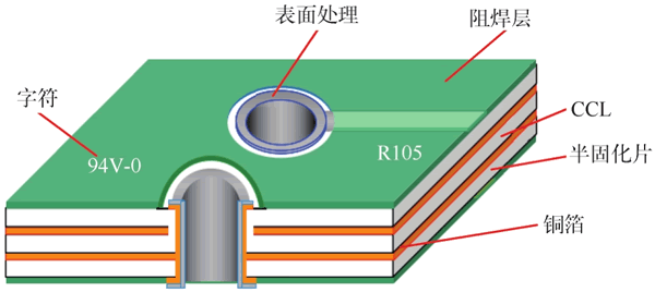
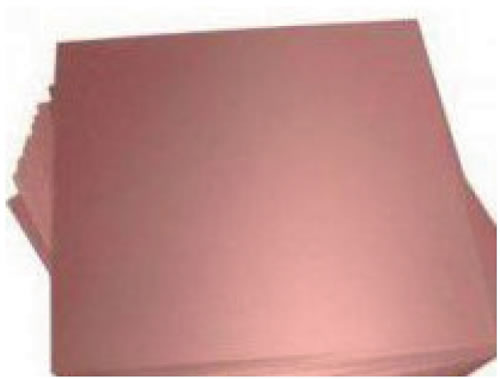
1) Copper Clad Laminate
Copper-clad laminate (CCL), referred to as copper-clad laminate or copper-clad laminate, is the basic material for manufacturing printed circuit boards. It is composed of a dielectric layer (resin, glass fiber) and a high-purity conductor (copper foil). composed of composite materials.
It was not until 1960 that professional manufacturers used formaldehyde resin copper foil as the base material to make single-sided PCBs, and put them into the market of record players, tape recorders, video recorders, etc. Later, due to the rise of double-sided through-hole copper plating manufacturing technology, heat resistance, size Stable epoxy glass substrates have been widely used so far. Nowadays, FR4, FR1, CEM3, ceramic plates and Teflon plates are widely used.
At present, the most widely used PCB made by etching method is to selectively etch on the copper clad board to obtain the required circuit pattern. The copper clad laminate mainly provides three functions of conduction, insulation and support on the entire printed circuit board. The performance, quality and manufacturing cost of printed circuit boards depend to a large extent on copper clad laminates
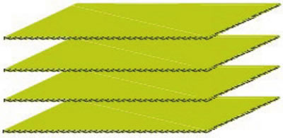
2) Prepreg
Prepreg, also known as PP sheet, is one of the main materials in the production of multilayer boards. It is mainly composed of resin and reinforcing materials. The reinforcing materials are divided into glass fiber cloth (referred to as glass cloth), paper base and composite materials.
Most of the prepregs (adhesive sheets) used in the production of multilayer printed circuit boards use glass cloth as a reinforcing material. The thin sheet material made by impregnating the treated glass cloth with resin glue, and then pre-baked by heat treatment is called prepreg. Prepregs soften under heat and pressure and solidify when cooled.
Since the number of yarn strands per unit length of the glass cloth in the warp and weft directions is different, attention should be paid to the warp and weft directions of the prepreg when cutting. Generally, the warp direction (the direction in which the glass cloth is curled) is selected as the short side direction of the production board, and the weft direction is The direction of the long side of the production board is to ensure the flatness of the board surface and prevent the production board from being twisted and deformed after being heated.
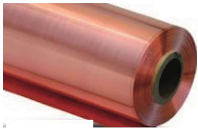
3) Copper foil
Copper foil is a thin, continuous metal foil deposited on the base layer of the circuit board. As a conductor of the PCB, it is easily bonded to the insulating layer and etched to form a circuit pattern.
Common industrial copper foils can be divided into two categories: rolled copper foil (RA copper foil) and electrolytic copper foil (ED copper foil):
Rolled copper foil has good ductility and other characteristics, and is the copper foil used in the early soft board process;
Electrolytic copper foil has the advantage of lower manufacturing cost than rolled copper foil
4) Solder mask
The solder resist layer refers to the part of the printed circuit board with solder resist ink.
Solder resist ink is usually green, and a few use red, black and blue, etc., so solder resist ink is often called green oil in the PCB industry. It is a permanent protective layer of printed circuit boards, which can prevent moisture, Anti-corrosion, anti-mildew and mechanical abrasion, etc., but also prevent parts from being welded to incorrect places.
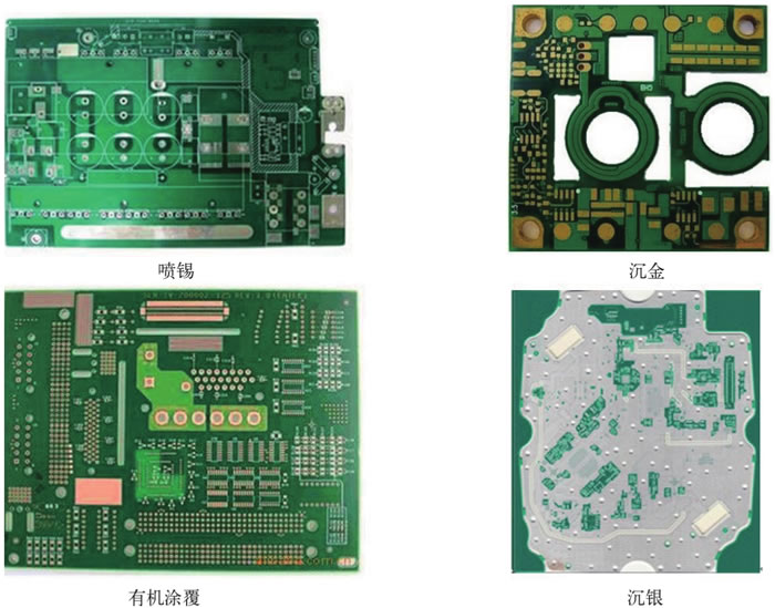
5) Surface treatment
“Surface” as used here refers to the connection points on the PCB that provide electrical connection between electronic components or other systems and the circuits on the PCB, such as connection points of pads or contact connections. The solderability of bare copper itself is very good, but it is easily oxidized and polluted when exposed to air, so a protective film should be covered on the surface of bare copper.
Common PCB surface treatment processes include lead HASL, lead-free HASL, organic coating (Organic Solderability Preservatives, OSP), immersion gold, immersion silver, immersion tin and gold-plated fingers, etc. With the continuous improvement of environmental protection regulations, there are The lead HASL process has been gradually banned.
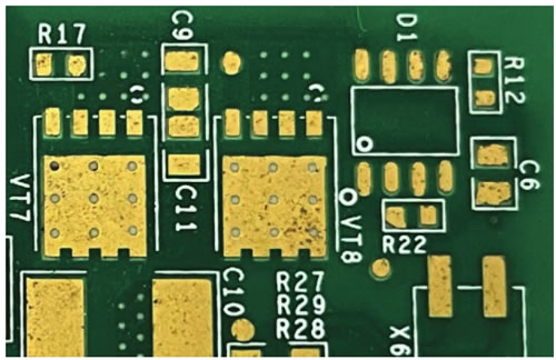
6) Characters
The character is the text layer, on the top layer of the PCB, it can be absent, and it is generally used for comments.
Usually, in order to facilitate the installation and maintenance of the circuit, the required logo patterns and text codes are printed on the upper and lower surfaces of the printed board, such as component labels and nominal values, component outline shapes and manufacturer logos, production dates wait.
Characters are usually printed by screen printing
Post time: Mar-11-2023