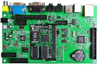
PCBA process: PCBA=Printed Circuit Board Assembly, that is to say, the empty PCB board passes through the SMT upper part, and then goes through the entire process of DIP plug-in, referred to as the PCBA process.
Process and Technology
Jigsaw join:
1. V-CUT connection: using a splitter to split, this splitting method has a smooth cross-section and has no adverse effects on subsequent processes.
2. Use pinhole (stamp hole) connection: It is necessary to consider the burr after the fracture, and whether it will affect the stable operation of the fixture on the Bonding machine in the COB process. It should also be considered whether it will affect the plug-in track and whether it will affect the assembly.
PCB material:
1. Cardboard PCBs such as XXXP, FR2, and FR3 are greatly affected by temperature. Due to different thermal expansion coefficients, it is easy to cause blistering, deformation, fracture, and shedding of the copper skin on the PCB.
2. Glass fiber board PCBs such as G10, G11, FR4, and FR5 are relatively less affected by the SMT temperature and the temperature of COB and THT.
If more than two COB. SMT. THT production processes are required on one PCB, considering both quality and cost, FR4 is suitable for most products.
The influence of the wiring of the pad connection line and the position of the through hole on the SMT production:
The wiring of pad connection lines and the position of through holes have a great influence on the soldering yield of SMT, because unsuitable pad connection lines and through holes may play the role of “stealing” solder, absorbing liquid solder in the reflow oven Go (siphon and capillary action in fluid). The following conditions are good for production quality:
1. Reduce the width of the pad connection line:
If there is no limitation of current carrying capacity and PCB manufacturing size, the maximum width of the pad connection line is 0.4mm or 1/2 pad width, which can be smaller.
2. It is most preferable to use narrow connection lines with a length of not less than 0.5mm (width not greater than 0.4mm or width not greater than 1/2 of the pad width) between pads connected to large-area conductive strips (such as ground planes, power planes).
3. Avoid connecting wires from the side or a corner into the pad. Most preferably, the connection wire enters from the middle of the back of the pad.
4. Through holes should be avoided as much as possible in the pads of SMT components or directly adjacent to the pads.
The reason is: the through hole in the pad will attract the solder into the hole and make the solder leave the solder joint; the hole directly close to the pad, even if there is a good green oil protection (in actual production, the green oil printing in the PCB incoming material is not accurate In many cases), it may also cause heat sinking, which will change the infiltration speed of solder joints, cause tombstoning phenomenon in chip components, and hinder the normal formation of solder joints in severe cases.
The connection between the via hole and the pad is most preferably a narrow connection line with a length of not less than 0.5mm (width not greater than 0.4mm or a width not greater than 1/2 of the pad width).
Post time: Feb-22-2023